
Electronics occupies a singular position in industrial inspection: it is the only field where the reference is perfectly known. The board to be produced exists as a design file, every component has a theoretical position, every trace an expected route. Comparing the product against its reference ought therefore to suffice.
The field’s datasets are built on exactly that principle. The reference corpus for bare boards contains 1,500 image pairs, each comprising a defect-free template image and a tested image of the same board at 640 by 640 pixels, with six annotated defect categories, open, short, mousebite, spur, pin-hole and spurious copper, and an average of three to twelve defect instances per tested image.
And yet template comparison is not enough. Manufacturing tolerances, variation in solder joint appearance and the diversity of component packages produce legitimate deviations that an overly strict system flags as defects. This article covers that tension, the inspection stages, the defect taxonomy and what it implies for annotation. It extends the complete guide to defect detection.
What sets electronics apart in defect detection
Three properties separate this vertical from every other one in defect detection, and they pull in opposite directions.An available reference
This single fact reshapes almost everything downstream, from how images are prepared to how quality is measured. Unlike wood or textile, the object inspected was designed. Design data provides the theoretical position of every component, its part reference, its orientation and the circuit layout. That information is usable in two ways: to generate inspection regions automatically, and to verify not merely that a component is present but that it is the right one.A demanding scale
The contrast with the preceding verticals is stark. The defects sought are measured in tens of micrometres on components some of which are under a millimetre. That scale demands high resolution, hence a small field of view, hence many acquisitions per board, with the stitching and cycle-time questions that follow. It also demands sufficient depth of field although the board is not flat, component heights varying widely.A large number of classes
Where a surface inspection handles five to ten classes, an assembled board inspection handles several dozen, spread across heterogeneous defect families. That ontological richness is the field’s primary source of complexity, and it drives annotation cost far more than image volume does.Inspection stages and their specific defects
An assembly line has several successive inspection points along its length, each seeing defects the others cannot. A defect detection project must state which stage it addresses, otherwise the ontology mixes incomparable objects.The bare board
Four stages matter, and they see different things. Before any component is placed, inspection concerns the etched circuit itself. The authors of a corpus dedicated to this stage note that existing public datasets do not cover it: they focus primarily on finished boards and often include soldering and component-mounting information, which fails to reflect the characteristics of early-stage defects in the manufacturing process. Their corpus targets three typical bare board defects: short circuit, open circuit and hole deviation.Solder paste
Catching problems here is cheaper than catching them anywhere downstream. After printing and before any placement, inspection concerns the paste deposits: volume, area, offset, bridging. This is the most cost-effective preventive stage, since a defect caught here is corrected without removing a component. It belongs to volumetric measurement more than to recognition, which points towards three-dimensional sensors.After placement and reflow
This is the stage richest in classes and best covered by optical systems. The technical principle rests on multi-angle coloured lighting: automatic optical inspection operates on machine vision principles, employing red, green and blue sources to illuminate components, and exploiting optical reflection to depict the soldering condition of components. Each angle of incidence is tied to a colour, which allows the local slope of the solder meniscus to be inferred from the observed colour.Electrical test and its complementarity
A scoping remark is needed: not every non-conformity belongs to vision. Electrical test detects functional faults no image reveals, and conversely vision detects appearance defects that have not yet produced an electrical failure but compromise long-term reliability. The two approaches are complementary rather than competing, and a vision-based defect detection project must state what it does not cover, otherwise expectations are built on a misunderstanding.Radiography
The final stage in the chain, and the only one that sees beneath components. Some defects are optically invisible: voids under the joint, solder beneath the component body, insufficient fill. They require transmission imaging. This stage brings its own annotation difficulties, notably locating regions of interest. One study notes that the joint of interest is located on the X-ray image by a region of interest and then inspected by algorithms, and that incorrect regions of interest deteriorate the inspection algorithm. Part of the error therefore originates in the framing step rather than in the decision.The defect detection taxonomy
The vocabulary of defect detection in electronics is settled and structured by family, which greatly eases ontology construction.Circuit defects
On the bare board and its traces, the taxonomy is purely geometric: trace interruption, unintended connection between two traces, local thinning by mousebite, copper protrusion, perforation in a pad, isolated copper residue. These six categories cover the essentials and have the advantage of being definable unambiguously by comparison with the theoretical layout, which makes them the easiest part of the field to annotate.Solder defects
They form the largest category in assembly by volume and the trickiest to annotate. A recent synthesis lists them: solder bridges, meaning unwanted conductive connections between adjacent pads, insufficient solder, meaning inadequate joint volume, cold joints, resulting from incomplete reflow and showing a dull granular surface, and solder balls displaced from the joint area.Placement defects
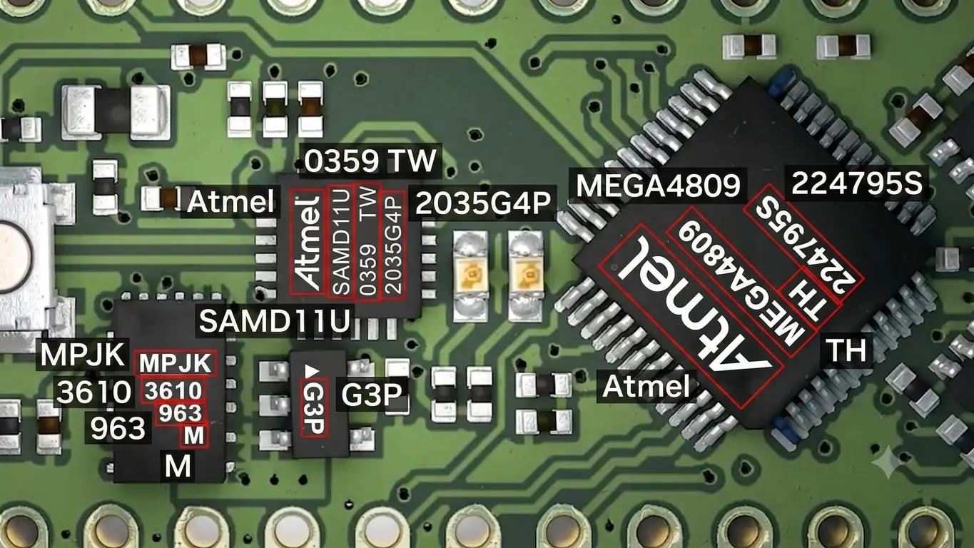
The second major family is tied to the placement machine rather than the oven. The same source lists the placement-related defects: missing component, component misaligned beyond tolerance, wrong component in value or package, and tombstoning where one end lifts during reflow under unbalanced surface tension. This family has a useful operational particularity worth exploiting: several of its classes are verified against design data rather than by appearance. A wrong component is detected by comparing the reference read from the marking with the expected one, which belongs more to character recognition than to visual defect detection.Ambiguous boundaries
This is the most important point for annotation, and it is explicitly documented: each defect class has a distinct visual signature, but the boundaries between classes, particularly between misalignment and tombstoning in early-stage images, require fine-grained classifiers to resolve reliably. The same source flags a second difficulty: classifiers must distinguish these morphologies not only from each other but also from the visual artefacts of conforming joints with atypical pad geometries or component orientations. Part of the work therefore consists of learning what is normal but unusual, which is exactly the kind of case annotators handle badly without an illustrated protocol.Normative reference standards
Electronics enjoys an advantage few domains have: a widely shared acceptability standard, tiered by product class according to the required level, from consumer electronics to critical applications. That inheritance has two practical consequences. First, the annotation ontology benefits from adopting the normative vocabulary rather than inventing one, which eases acceptance by inspectors and avoids a later mapping exercise. Second, acceptance criteria already exist in written and illustrated form, providing a protocol base markedly better than what most other verticals have. One important caveat applies to reusing them directly. Those criteria are written for a human inspector with a microscope who can vary their viewing angle. Transposing them to a fixed image requires translation work, particularly for criteria involving three-dimensional judgement such as wetting or fillet angle. That work belongs to project scoping and cannot be delegated to annotators.Annotation in electronic defect detection
The availability of a reference changes the nature of annotation work and enables substantial savings. Three consequences follow. The first concerns localisation. The regions to inspect do not have to be found at all: they are derived from design data. An annotator therefore does not scan an image looking for anomalies, they examine a series of crops each corresponding to an identified joint or component. That arrangement sharply reduces unit cost and permits far more rigorous control, since the list of objects to examine is known in advance. The second concerns the metadata that must be retained alongside each label. Every annotation must be tied to the component designator, its part reference and its package. That information then allows performance to be analysed by package type, which is the field’s most informative breakdown: a system can be excellent on standard-size passives and mediocre on ball grid arrays or fine-pitch components. The third concerns the choice of annotation primitive. On a crop centred on a joint, classification is usually sufficient, which is markedly cheaper than segmentation. Delineation is justified only for extended defects such as bridges, or where measurement enters the decision rule.The cost of an electronic inspection project
The cost profile of this vertical differs markedly from the others, in a rather favourable direction. The dominant cost line is not image traversal, since inspection regions are generated automatically, nor delineation, since crop-level classification often suffices. It is twofold: building the ontology and its example plate, which must cover dozens of classes multiplied by package families, and arbitrating boundary cases, which mobilises a quality technician. That structure has a scoping implication. A project covering few classes across many images costs proportionally little; a project covering the full normative class list across a varied package population costs a great deal, regardless of volume. Restricting scope to the classes actually encountered on the line, rather than importing an entire standard, is the main saving available.The role of design data
Exploiting design data is the defect detection lever most specific to this vertical, and it is often underused. Three uses stand out, and they compound rather than substitute for one another. Automatic generation of regions of interest, which removes a substantial part of manual preparation. Consistency checking, where the system verifies not an appearance but a correspondence between what is mounted and what should be. And corpus stratification, where knowing the package guarantees each family is represented. That exploitation does presuppose preliminary alignment work between the design coordinate frame and the image, an operation whose reliability governs everything else. A systematic offset of a few pixels in that alignment produces poorly centred crops and annotations that look inconsistent when the problem is purely geometric.Public datasets and their incompatibility
The field has several public defect detection datasets, but combining them runs into a documented obstacle. The obstacle is one of representation rather than of content. One analysis notes that some corpora use black-and-white images where others employ colour representation, and this difference in imaging method and image representation affects dataset compatibility and usability, and consequently model training and performance. The same analysis identifies two more general limits: existing methods struggle to maintain accuracy in the face of manufacturing variability, variations in layout, component placement and soldering conditions, and they adapt poorly when deployed in different manufacturing environments or confronted with defect types absent from training. The practical conclusion matches that of the other verticals: these datasets serve for familiarisation and prototyping, not for estimating performance. A corpus specific to the line, covering its boards, packages and soldering conditions, remains indispensable.Board diversity as a structuring factor
An assembly line rarely produces a single board reference, and that diversity raises a problem other verticals encounter less. The consequence compounds quickly. Every new board introduces a different layout, a partly new component set and sometimes packages never seen before. A system learned board by board becomes unmanageable past a dozen references. A system learned at joint or component level, by contrast, transfers: a capacitor in a given package solders the same way whatever board carries it. That single observation strongly shapes corpus design and is worth acting on early. The relevant annotation unit is not the board but the component or the joint, and stratification should be by package type rather than by board reference. A corpus built on that basis naturally covers new boards as long as they use already represented packages, which is the common case.False calls, the central economic problem of electronic defect detection
In this vertical, the balance between escapes and false rejects takes a particular form that must be understood to scope a project correctly. The reasoning deserves setting out numerically. A single board carries thousands of inspection points. Even a very low false call rate per point produces, at board level, a non-negligible probability that at least one point is flagged wrongly. Every flag generates a manual verification, and the cumulative cost of those verifications is often the dominant inspection expense. Two annotation consequences follow directly from that arithmetic. First, the corpus must contain large numbers of conforming joints, including atypical ones, since their diversity determines the false call rate. Second, the expected output is better as a score than as a decision, so that flagged points can be presented to the operator in decreasing order of suspicion, which sharply reduces verification time.Quality control of electronic defect detection annotation
Annotation in electronic defect detection requires particular expertise, but not the kind one might assume. Role allocation is more favourable than supposed. Distinguishing a conforming joint from an insufficient one, recognising the dull surface characteristic of a cold joint, spotting incipient tombstoning: these are visual recognition acts and delegate well to trained annotators, provided the example plate covers the range of normal appearances per package. The quality technician’s expertise comes in on defining acceptance thresholds, arbitrating boundary cases and validating the protocol. Control must accordingly be stratified by package type and by defect class, difficulty varying considerably between a large passive component and a ball grid array. One further practice helps: measuring agreement separately on atypical conforming joints, which are the main source of false calls and whose correct annotation governs the system’s economic performance.Handling new component packages
One operational question recurs and deserves planning for: what happens when a package appears that the corpus does not cover. The naive answer, retraining the whole model on everything, is both slow and disproportionate. A better arrangement treats new packages as a routine event with a defined path: the system flags points it cannot assess with confidence rather than guessing, those points route to manual verification, and the resulting images feed a small targeted annotation campaign. The model is then extended rather than rebuilt. That arrangement requires two things decided at design time. The model must be able to express low confidence rather than always producing a class, and the annotation pipeline must be able to absorb small frequent batches rather than only large ones. Neither is difficult to build in from the start; both are painful to retrofit.The most common mistakes
These failures recur often enough across electronic inspection projects that naming them is usually enough to avoid them.- Building an ontology mixing defects seen at different inspection stages.
- Not tying each annotation to the component designator, part reference and package.
- Neglecting validation of the alignment between design data and images.
- Expecting optical inspection to catch internal defects that require radiography.
- Under-representing atypical conforming joints, the main cause of false calls.
- Not explicitly distinguishing misalignment from tombstoning in the protocol.
- Combining public datasets with incompatible image representations.
- Delivering a binary decision instead of a score usable to triage verifications.
- Controlling quality globally rather than stratifying by package type.